More Routing Density
Additional copper layers create more routing channels without expanding the board outline. This can help accommodate fine-pitch components, connectors, memory, and complex interface groups.
GlobalWin reviews multilayer PCB manufacturing requirements from layer count and FR-4 materials to controlled impedance and testing. Plan signal, power and ground layers as one stackup before requesting a technical quote.
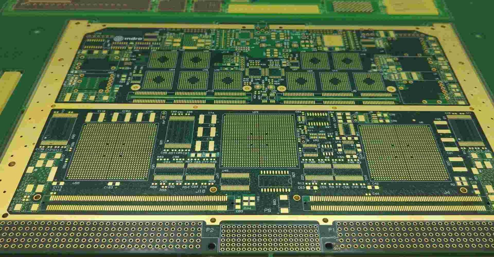
Quick answer: A multilayer PCB is a printed circuit board made from three or more conductive copper layers separated by insulating dielectric material. It is used when a two-layer board cannot provide enough routing area, reference planes, power distribution, or signal-integrity control.
The correct layer count is not determined by component count alone. It should be selected through stackup planning, routing analysis, impedance requirements, thermal considerations, manufacturability, and the target cost of the product.
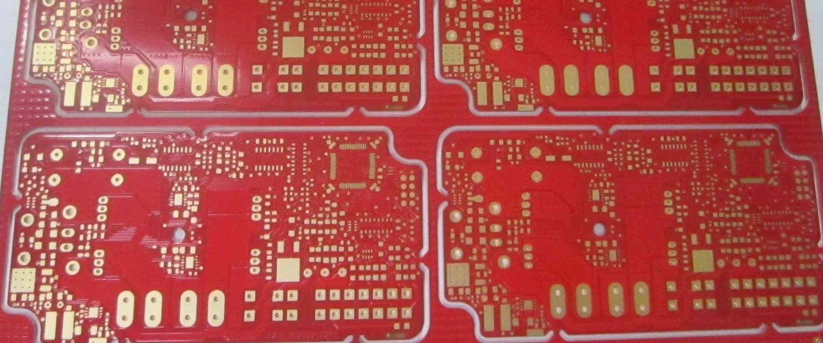
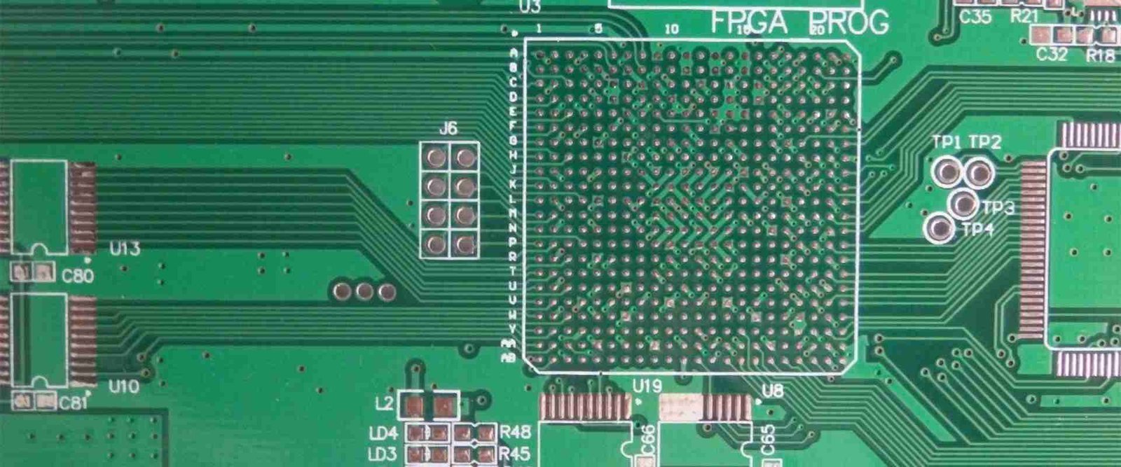
Multilayer construction is usually considered when the design needs more electrical or mechanical control than a single-sided or double-sided board can provide.
Additional copper layers create more routing channels without expanding the board outline. This can help accommodate fine-pitch components, connectors, memory, and complex interface groups.
Dedicated or semi-dedicated planes can support power distribution, return-current planning, thermal paths, and more controlled separation between functional circuits.
A planned stackup can place high-speed signals close to reference planes and support controlled-impedance routing for selected nets.
Layer expansion can provide more circuit functionality within a restricted enclosure, provided thermal, assembly, and service requirements remain achievable.
Analog, digital, power, RF, and control sections can be organized with clearer layer and return-path strategies during layout review.
A stable stackup and documented fabrication package can make the transition from prototype builds to repeat production more predictable.
Layer count should be chosen from the design constraints rather than from a standard number. The table below is a planning guide; the final layer count should be confirmed after layout and stackup review.
Layer counts here are planning examples. No 32-layer manufacturing capability is implied by this guide.
The same layer count can perform differently depending on board size, copper distribution, dielectric geometry, via structure, and routing strategy.
| Layer Count | Typical Design Direction | Main Review Points |
|---|---|---|
| 4-layer PCB | A practical starting point for moderate routing density, basic power distribution, and improved reference-plane planning. | Plane allocation, return paths, copper balance, board thickness, and whether all interfaces can be routed without excessive vias. |
| 6-layer PCB | Provides additional routing capacity and more flexibility for signal, power, and reference-layer assignment. | High-speed net placement, plane continuity, controlled impedance, via transitions, and signal grouping. |
| 8-layer PCB | Often considered for dense digital systems, multiple interfaces, fine-pitch packages, and more demanding signal-integrity goals. | Stackup symmetry, impedance coupons, BGA escape routing, crosstalk control, power distribution, and thermal management. |
| 10-layer PCB and above | Supports complex designs that require substantial routing area, multiple reference structures, and functional separation. | Lamination construction, registration, aspect ratio, fabrication yield, total thickness, material availability, and test coverage. |
On smaller screens, scroll this table horizontally to compare all columns.
Layer-count guidance is not a substitute for a project-specific stackup. Final recommendations depend on the fabrication data, component package, electrical targets, and mechanical constraints.
The stackup determines how copper layers, dielectric materials, reference planes, and controlled-impedance structures work together. It should be reviewed before fabrication data is released.
This is an explanatory concept, not a production stackup. Actual dielectric thickness, material system, copper weight, impedance geometry, and finished thickness must be confirmed for each project.
Standard FR-4 is suitable for many general-purpose multilayer designs. High-Tg, low-loss, halogen-free, and other laminate systems may be considered when the design has higher thermal, electrical, environmental, or compliance requirements.
| Material Direction | When It May Be Considered |
|---|---|
| Standard FR-4 | General industrial, consumer, control, and embedded electronics where standard thermal and dielectric performance is acceptable. |
| High-Tg FR-4 | Designs with higher operating temperatures, demanding assembly profiles, or increased thermal margin requirements. |
| Low-loss laminate | High-speed or high-frequency designs where dielectric loss, propagation behavior, and signal-integrity targets require additional consideration. |
| Halogen-free materials | Products with specific material declarations, environmental goals, customer requirements, or regional compliance needs. |
On smaller screens, scroll this table horizontally to compare all columns.
A multilayer PCB is more predictable when the electrical design, stackup, fabrication process, and inspection plan are reviewed together.
Confirm the layer sequence, dielectric construction, copper weight, finished thickness, symmetry, and material availability before releasing the fabrication package.
Identify impedance-controlled nets, target values, tolerance, reference planes, trace geometry, and whether test coupons are required.
Review plane continuity, current paths, decoupling strategy, copper distribution, thermal spreading, and return-current behavior.
Check plated through holes, blind or buried vias, backdrilling, via-in-pad requirements, annular ring, clearances, and drill registration.
Review spacing, copper balance, solder mask openings, board edge features, slots, tooling, panelization, and manufacturing risk.
Align Gerber or ODB++ data, drill files, fabrication drawing, stackup notes, revision information, special requirements, and acceptance criteria.

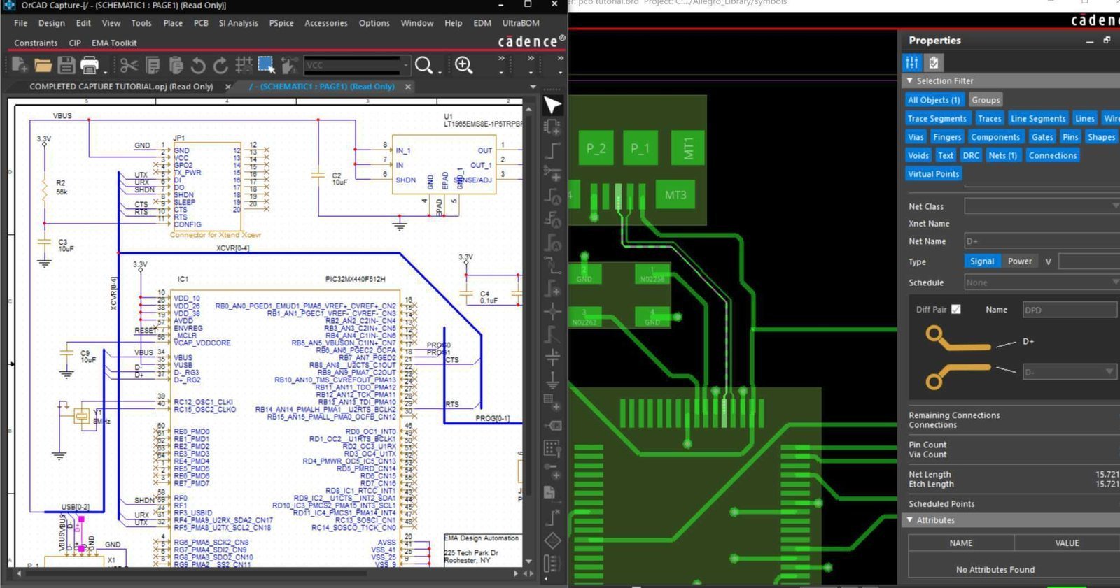
Each project should be quoted against its actual fabrication data. The following items identify the technical information normally reviewed for a multilayer PCB build.
Do not select a generic capability value when the design has controlled impedance, fine-pitch packages, heavy copper, unusual thickness, or special via structures.
| Parameter | Engineering Considerations | Confirmation Basis |
|---|---|---|
| Layer count | Number and function of signal, power, and reference layers. | Layout density, interfaces, plane strategy, and final stackup. |
| Finished board thickness | Affects mechanical fit, dielectric geometry, via aspect ratio, and impedance calculations. | Mechanical drawing, enclosure, connector, and assembly requirements. |
| Inner and outer copper | Influences current capacity, thermal behavior, etching, plating, and copper balance. | Current requirements, thermal analysis, and fabrication drawing. |
| Trace and space | Must be evaluated together with copper thickness, layer type, component pitch, and yield expectations. | Gerber, ODB++, IPC-2581, or other accepted fabrication data. |
| Impedance control | Requires defined targets, tolerances, reference planes, dielectric data, and trace geometry. | Impedance table, stackup, net list, and approved calculation. |
| Via structures | Through vias, blind vias, buried vias, backdrilled vias, microvias, and via-in-pad each affect cost and process risk. | Drill files, padstack data, aspect ratio, and DFM review. |
| Surface finish | Selection affects solderability, flatness, contact performance, storage, and assembly requirements. | Assembly process, exposed contacts, product life, and customer specification. |
| Testing and inspection | Inspection coverage may include AOI, electrical test, impedance verification, microsection, and dimensional checks. | Product risk, IPC class, drawing requirements, and quality plan. |
On smaller screens, scroll this table horizontally to compare all columns.
Final values, tolerances, material brands, and process availability should be confirmed in the project quotation and approved fabrication documentation.
Multilayer fabrication depends on accurate inner-layer imaging, controlled lamination, reliable interconnection, and inspection at the appropriate process stages.
Confirm design files, board outline, stackup, drill data, materials, special features, and manufacturing constraints.
Transfer the inner-layer circuit pattern to the selected copper material and prepare the layers for etching and inspection.
Form the inner circuits and inspect the patterned layers before the lamination package is assembled.
Assemble cores, prepreg, and copper foils according to the approved stackup, then bond them into a multilayer panel.
Create plated and non-plated holes, followed by desmear and preparation for reliable interlayer connection.
Build the required copper connection and form the outer-layer circuitry according to the approved fabrication data.
Apply solder mask, legend, and the selected surface finish based on assembly, contact, reliability, and storage requirements.
Complete the agreed inspection and test plan, review documentation, package the boards, and prepare them for delivery.
Quality planning should reflect the risk profile of the board. High-density multilayer designs benefit from inspection that covers both visible features and internal interconnections.
Review inner-layer patterns before lamination to identify opens, shorts, missing features, and pattern issues.
Check relevant outer and inner features, solder mask, silkscreen, surface finish, and visible workmanship.
Select flying probe, fixture-based electrical testing, or another agreed method according to quantity and requirements.
Verify controlled-impedance structures when targets, coupons, and acceptance tolerances are defined in the documentation.
Use cross-section analysis when the project requires evidence of plating, hole quality, copper thickness, or lamination.
Confirm board outline, hole locations, thickness, slots, edge features, and other mechanical requirements.

Clear answers to common questions about multilayer PCB design, materials, impedance, files, and inspection.
A multilayer PCB is a printed circuit board made from three or more conductive copper layers separated by dielectric material and bonded into one board. The additional layers provide more routing area and allow dedicated power or ground planes.
The required layer count depends on routing density, component package, signal speed, power distribution, impedance targets, thermal requirements, and board size. Four or six layers may suit moderate designs, while dense or high-speed systems may require eight or more layers.
Common material systems include standard FR-4, high-Tg FR-4, low-loss laminates, and halogen-free materials. The correct choice depends on operating temperature, dielectric requirements, signal frequency, compliance needs, and cost targets.
Yes. Controlled impedance can be designed through the relationship between trace geometry, copper thickness, dielectric thickness, dielectric constant, reference planes, and the selected stackup. The target impedance and relevant nets should be defined during the engineering review.
A typical quote package includes Gerber or ODB++ files, NC drill files, a fabrication drawing, board outline, layer build information, material requirements, surface finish, copper weights, quantity, and target delivery information.
Inspection may include inner-layer and outer-layer AOI, electrical testing, dimensional inspection, solder mask and surface finish checks, impedance verification, microsection analysis, and other tests selected according to the design and purchase requirements.
Share your fabrication files, quantity and assembly requirements.